Technology
Our 3-D Solar Carbon Nanotube Array is the future for inexhaustible energy collection.
Low efficiency and high cost render current silicon technology unable to satisfy ever-rising electricity demands. Flat silicon panels (considered "2-D") reflect rather than absorb most photons, limiting their efficiency to an average of 15-20%.
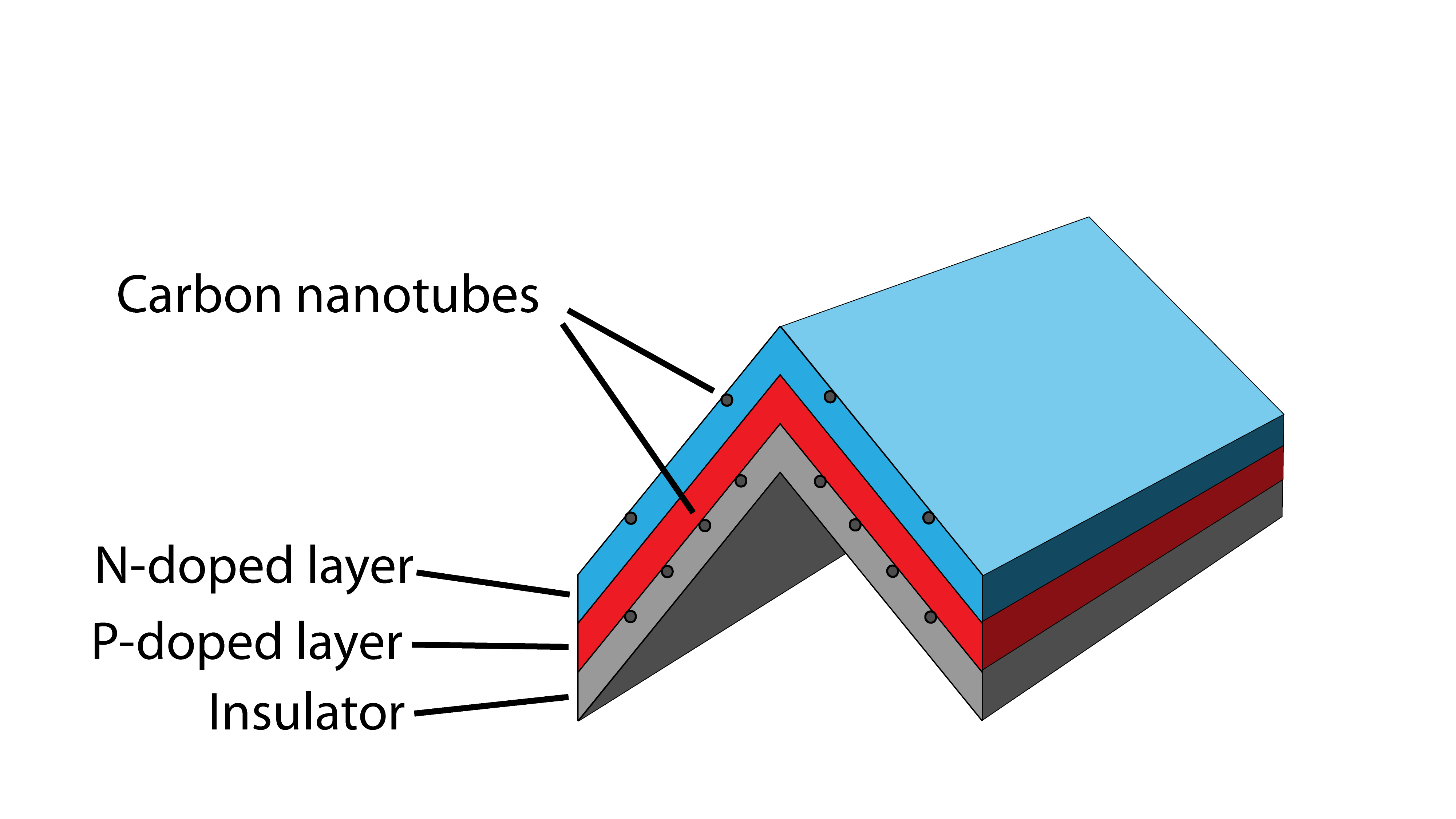
Our array uses newly designed nano-ridge structures to allow photons to "bounce" between them, increasing efficiency. New materials enhance photon collection and the array's integrity.
Components and Properties
Carbon Nanotubes
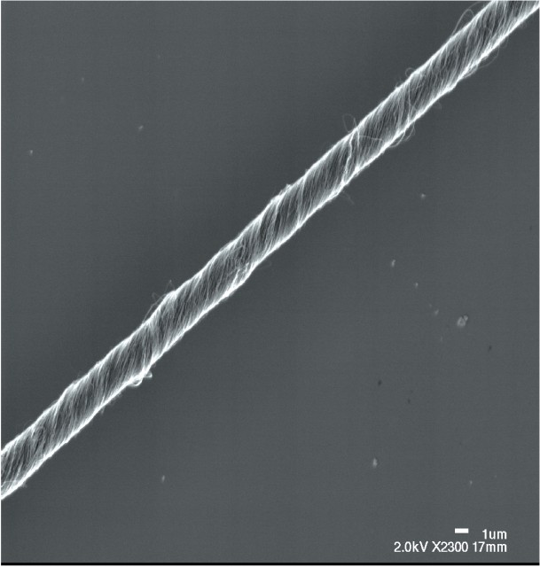
Single wall carbon nanotubes (SWNT) possess useful properties along with their conductivity. At 1/6 the weight and 100 times stronger than steel, they reinforce the array, boosting weather resistance.
Nanotubes take up less space than silver contacts, providing more surface area for photon collision.
The Semiconductor Indium Gallium Nitride (Red P-Doped, Blue N-Doped)
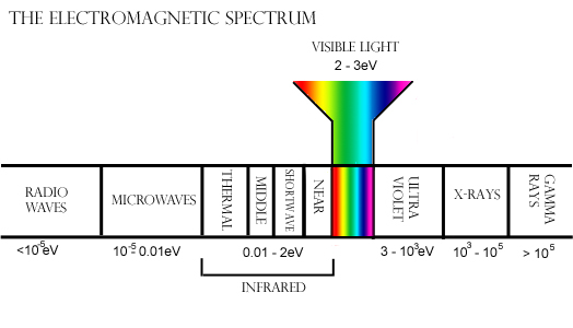
InGaN is a superb replacement for the silicon used in most panels today. Its larger band gap (1.1 - 3.4 eV) compared to that of silicon (1.1 eV) allows an almost complete conversion of the full spectrum of sunlight into electrical current. Our novel geometry boosts theoretical efficiencies from 70% to near 86%, the highest possible conversion rate due to photon entropy.
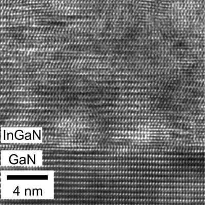
Metal modulated epitaxy, a recent breakthrough in semi-conductor production, grows atom-thick layers of indium gallium nitride (InGaN) one by one. This creates a near-perfect crystal lattice, allowing for consistency of the individual elements in the semiconductor while boosting efficiency. It's also a low-cost material used in LEDs today.